
Introduction
Every hour, the sun gives the Earth approximately 1.7 × 10¹³ joules of energy, which is even more than what all humans consume in a whole year. Though, capturing and converting this large amount of energy in an efficient and cost-effective manner has always been the main issue in the use of solar energy. Traditional silicon solar cells, which are mainly used in the market, are limited by the Shockley-Queisser limit to a maximum efficiency of about 33% for a single-junction device under one sun illumination; in fact, commercial silicon panels usually achieve efficiencies of around 20–22%. The difference between what is theoretically possible and what is achieved in the real world is the reason for a large-scale research program in both fundamental and applied areas, and nanoscience, in particular, has emerged as a very productive area of this research.
Nanotechnology in solar energy may well have started with an experiment in 1991, when a mesoporous film of anatase TiO2 nano crystallites coated with a monolayer of ruthenium dye by O’Regan and Grätzel could be converted to energy at a rate of 7.1 – 7.9% at a very low cost a result which helped molecular and nanoscience to be firmly established in photovoltaics (1). Since then, this area of work has become extremely studied. Quantum dot solar cells, perovskite nanocrystal devices, plasmonic architectures, and nanofluid-enhanced thermal collectors have individually undergone from physics study driven by curiosity to technologies that are now commercially viable each. This perspective seeks to highlight the main issues which will determine whether or not nanotechnology can bring about the solar energy revolution that it has been promising all along.
Dye-sensitized solar cells and the nanostructured photoanode
The dye-sensitized solar cell (DSSC) crafted by O’Regan and Grätzel (1) was the very first realization of a concept that nanoscale architecture could be used to get around the limits of planar semiconductor junctions. The main breakthrough was topological: instead of a flat TiO2 film, a three-dimensional, interconnected network of ∼20 nm nanocrystallites was created so that the surface area available for dye adsorption is increased one thousand times or even more relative to the projected geometric area. The single-molecule sensitizer layer is able to capture a large part of the solar spectrum, despite each dye molecule only absorbing light very weakly.
A dye anchored for a DSSC, upon absorbing a photon, gets excited, and an electron is promptly (within femtoseconds) released to the TiO2 NP’s conduction band (Figure 1) via electron injection. The electron goes through the nanocrystalline network to the transparent conducting electrode, while the dye that gained a positive charge is restored by a redox mediator (typically the iodide/triiodide couple) diffusing through the electrolyte. Even though DSSCs have not replaced silicon in high-power applications, they are still relevant for building-integrated photovoltaics, portable electronics, and as the intellectual initiators of the much more efficient perovskite solar cell. Swapping the ruthenium dye for organic or porphyrin sensitizers, exchanging liquid electrolytes for solid-state hole-transport materials, and producing one-dimensional TiO2 nanotubes or nanowires for faster electron transport have all given rise to gradual but significant improvements.
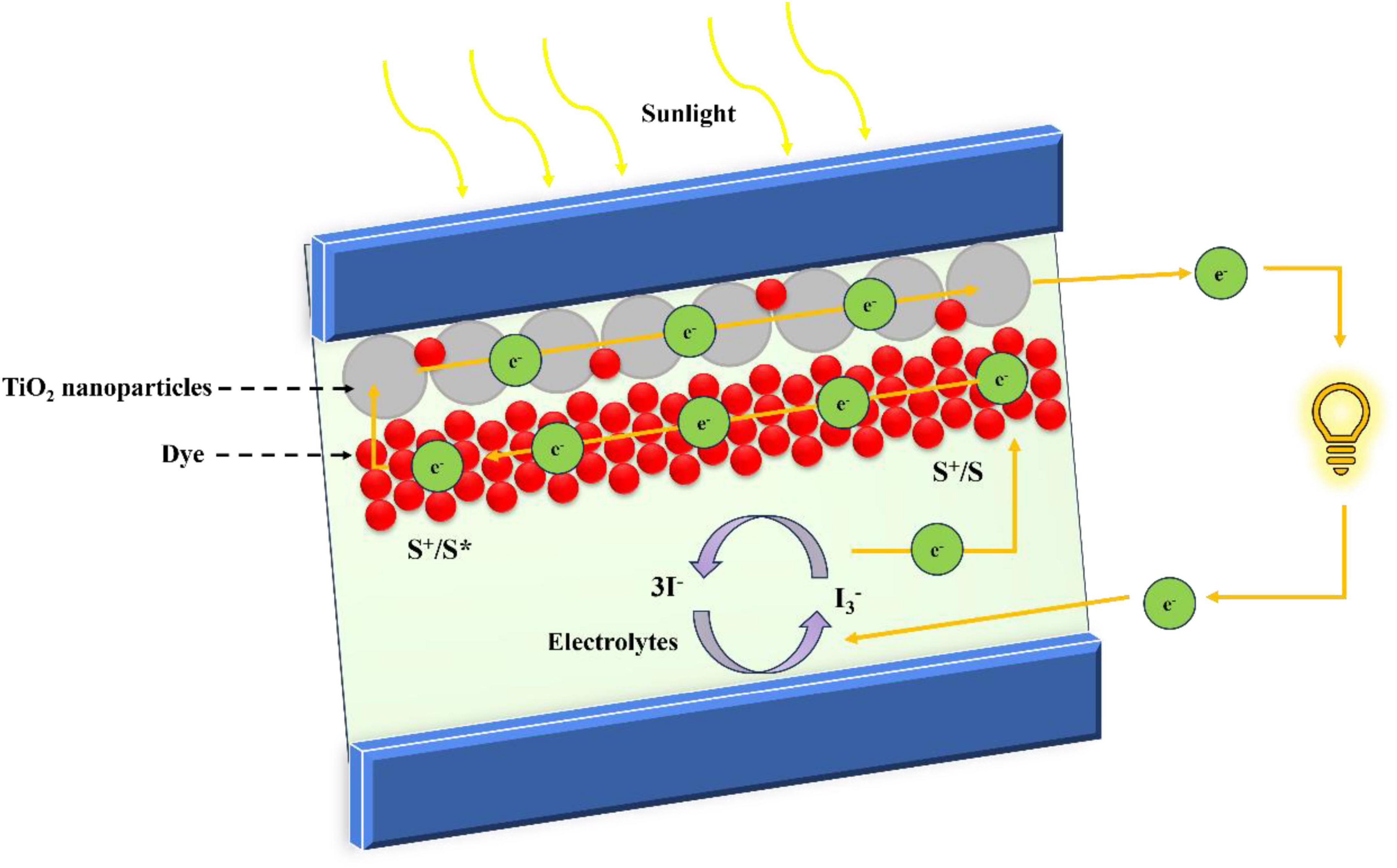
Figure 1. Schematic illustration of dye-sensitized solar cells (DSSC) and the nanostructured photoanode.
Quantum dot photovoltaics and multiple exciton generation
Semiconductor quantum dots (QDs) are colloidal nanocrystals with a less than nanometer made of materials such as PbS, PbSe, CdSe, or InP. They demonstrate quantum confinement most effectively. Since the de Broglie wavelength of electrons and holes in these materials is almost equal to the particle size, the energy levels of electrons become discrete and can be tuned to the size of the particle. For example, a QD made of PbS with a diameter of 3 nm absorbs light in the visible region mainly, yet a particle of 6 nm size absorbs light well into the near-infrared region. Due to this spectral flexibility, it is possible to set the absorption onset of a solar cell by changing the nanocrystal size during colloidal synthesis without changing the chemical composition, as shown in Figure 2. On top of the bandgap engineering, QDs present a way that is not available in bulk semiconductors, which is the generation of multiple excitons (MEG), or carrier multiplication. It is well known that when a photon is absorbed by a bulk semiconductor, its energy being much higher than the bandgap energy, the excess energy is converted to heat very fast through phonon emission. Still, due to quantum confinement, they not only slow down the phonon relaxation but also increase the Coulomb interaction between carriers. As a result, one single high-energy photon can generate two or more electron/hole pairs. Nozik and his group came up with a detailed theory and experiments on MEG and showed that the solar cell efficiency could be quite a bit higher than the Shockley-Queisser limit if this process is fully exploited (2). MEG quantum yields higher than 100%, meaning more than one electron per photon, have been reported in PbSe and PbS QD systems.

Figure 2. Schematic illustration of QD photovoltaics and multiple exciton (MEG) generation.
QD solar cells have come a long way since the first Schottky-junction-type cells in the mid-2000s. The best PbS QD solar cells recently certified to convert sunlight to electricity have a power conversion efficiency of about 13–14%, which has been possible due to various improvements. Some of these improvements were ligand engineering for good passivation of the surface traps, fabrication of depleted heterojunction structures, and recently, taking advantage of the coupling of QDs in ordered superlattices to enhance charge transport. Though these efficiencies are still far below those of perovskite or silicon cells, QD solar cells are ideal for applications where near-infrared absorption, mechanical flexibility, or low-temperature solution processing are required.
Perovskite nanocrystals cells: a paradigm shift
What happened with organic-inorganic halide perovskite solar cells possibly eclipsed all other innovations in photovoltaic technology for speed and scale of transformation (Figure 3). The four researchers Kojima, Teshima, Shirai, and Miyasaka discovered in 2009 that the methylammonium lead halide perovskite materials, if arranged in the form of nanocrystals on a mesoporous TiO2 matrix, could be used as visible-light sensitizers exhibiting a photovoltage of 0.96 V (3). The performance levels in the beginning were quite low. Today, solar cells based on a single-junction perovskite with efficiency levels that have been independently verified at over 26% and perovskite-silicon tandem devices have reached 34.6% (4).

Figure 3. Schematic illustration of perovskite nanocrystal solar cells.
Nanotechnology is involved at every step of this game-changer. The perovskite layer acting as an absorber is in fact a nanostructure in itself. Films formed by the solution process are made up of crystalline grains measuring 100–500 nm, and performing the defect passivation on grain boundaries with the help of functional organic molecules or inorganic nanosized particle layers is now a very common method for reaching radiative efficiency limits (5). Reliability is the main issue with perovskites that prevents their commercial use. The normal form of methylammonium lead iodide breaks down when it comes into contact with moisture, oxygen, heat, and ultraviolet light. Nanoengineering methods of dealing with this issue include enclosing perovskite grains in hydrophobic shell materials, replacing the volatile methylammonium cation with formamidinium or mixed composition, and reducing the dimensions to two-dimensional perovskite nanostructures that provide a higher degree of tolerance to humidity.
Plasmonics: light management at the nanoscale
Light interaction with metallic nanostructures leads to localized surface plasmon resonances (LSPRs), which are plasma oscillations of conduction electrons in metal that enable concentration of electromagnetic energy in volumes that are subwavelength and dramatically smaller than the wavelength of light (6). Atwater and Polman pointed out that this property could be used to enhance the absorption of sunlight in photovoltaic cells, mostly in thin-film solar cells where the absorber layer is too thin to absorb all the sunlight in just one pass. They reviewed the subject and listed three ways in which plasmonic enhancement can work: using the plasmonic nanoparticles to scatter the incident light in such a way that the light path inside the active layer of the solar cell is increased; using the near-field plasmonic enhancement to create a large local photon density of states very close to the nanoparticle; and using the absorbed photons to create “hot electrons” which can be injected across a metal semiconductor junction.
In their work, Catchpole and Polman established the main design rules that control the scattering by plasmonic nanoparticles near their resonance condition. They showed that particle shape, particle environment, dielectric constant, and particle position inside the device layers are all important influencing factors (7). Silver nanoparticles incorporated in the rear reflector of an amorphous silicon solar cell were identified as giving path-length enhancements comparable to those achieved by state-of-the-art random textures. It has also been shown that by engineering gold nanorod arrays, nanoshells, and core-shell structures, one could favor the scattering of light into guided modes of the absorber layer, and bimetallic nanoparticles persistently provide wider spectral coverage than those made from a single metal component. Researchers found that in perovskite solar cells, plasmonic nanoparticles can be introduced into the electron transport layer, hole transport layer, and even inside the perovskite film. So, the source of the combined benefits is through the improvement of light absorption, the near-field enhancement of functions related to exciton generation, and in some cases, the nanoparticle ligand shell-mediated passivation of recombination sites.
Nanofluids for solar thermal energy conversion
Solar energy conversion extends beyond photovoltaics alone. Solar thermal equipment like flat-plate collectors, evacuated tube collectors, and concentrated solar power plants harness the sun’s rays to produce hot water, heat for industrial use, and large-scale electricity generation through steam cycles. The thermodynamic efficiency of these devices depends largely on the heat transfer capabilities of the operating fluid. Choi and Eastman in 1995 were the first to suggest that suspending tiny metal or metal oxide particles in a standard heat transfer fluid creates “nanofluids” with remarkably improved thermal conductivities (8). Their theoretical forecasts have been experimentally verified for numerous combinations of nanoparticle and base fluids.
For solar thermal collectors, nanofluids are beneficial in two ways. Firstly, they enhance convective heat transfer between the absorber surface and the fluid, which lowers the thermal resistance and lets the collector run at a cooler absorber temperature while delivering the same amount of useful heat, resulting in better Carnot efficiency for any downstream thermodynamic cycle. Secondly, some nanoparticle suspensions like graphene nanoplatelets, gold nanoparticles, or carbon nanotubes can absorb solar energy in a “direct absorption solar collector” manner, entirely skipping the usual selective absorber coating (9, 10). Research has illustrated that using the optimal nanofluid mixtures can increase the thermal efficiency of flat-plate and evacuated-tube collectors by 15–32% (11) when compared to water, but the extent of the improvement depends heavily on factors such as the type of nanoparticle, size distribution, volume fraction, and the stability of the suspension over time.
Carbon-based nanomaterials as solar thermal media have received a lot of attention. Multi-walled carbon nanotubes (MWCNTs) have thermal conductivities of more than 3000 Wm–1K–1 in the direction of the tube, and graphene nanosheets have similar in-plane conductivities (12). These materials, when suspended in water or ethylene glycol, can create nanofluids that have thermal conductivities 15–25% higher than those of base fluids with volume fractions less than 0.5% (13). Besides thermal properties, carbon-based nanofluids also have very strong broadband optical absorption, which makes them excellent candidates for direct absorption collectors. The task of keeping colloidal stability, which means stopping irreversible aggregation that harms both optical and thermal properties, keeps researchers busy. Various ways include surface functionalization, pH control, and adding dispersants.
Carbon nanomaterials in photovoltaics
Carbon nanomaterials like single-walled carbon nanotubes (SWCNTs), graphene, and fullerenes have found a very unique spot in PV research. Their top-notch electrical conductivity combined with mechanical flexibility, abundance, and photostability have turned them into promising candidates for electrode materials and interfacial layers capable of replacing costly, scarce, or fragile traditional materials. Graphene, having near invisibility in the visible light spectrum coupled with a very high sheet conductance, naturally appears as a potential replacement for indium tin oxide (ITO) as the transparent electrode in flexible solar cells (14). Still, to be able to align chemically and energetically with neighboring transport layers, its work function and surface chemistry need to be meticulously modified.
In DSSC, extensive research has been done on carbon nanotubes and graphene nanoplatelets as alternatives to the platinum counter electrode, the latter being a catalyst for the regeneration of the iodide redox mediator at the cathode (15, 16). A thorough recent review established carbon-based counter electrodes are capable of matching the performance of platinum ones, with SWCNT electrodes having reached 7.79% and graphene nanoplatelets 9.3% power conversion efficiency in laboratory DSSC setups (15). Besides DSSCs, SWCNTs used as hole-selective transport layers in silicon heterojunction solar cells have led to efficiencies greater than 21%, without the need for boron-doping or inorganic passivation layers (17). These findings illustrate the various roles carbon nanomaterials can be entrusted with in the production of future photovoltaic devices.
Challenges, opportunities, and outlook
On the nanoscale, solar energy could help with great scientific discovery. But the shift from lab test results to stable, scalable, and reasonably priced commercial products is very challenging. Among the many issues, four main challenges stand out.
Reliable operation and long lifetime
Solar panels for commercial purposes typically come with a warranty of 25–30 years of outdoor use. Perovskite solar cells, the most efficient among the newer technologies, can degrade when exposed to a combination of light, moisture, and heat. Although using encapsulation methods and altering the chemical composition of the materials have much increased the operating lifetime, obtaining the level of financial reliability for supporting a large-scale project is still an open question. In the same way, colloidal QD solar cells suffer from the problem of ligands coming off and the QD surfaces getting oxidized. Creating guidelines for accelerating aging and setting up standardized stability testing procedures are indispensable for precision in measuring lifetimes and also for providing direction in material innovation.
The ability to scale and produce on a large scale
Most efficient perovskite solar cells are made by spin-coating on very small substrates in very controlled laboratory environments. Going to a very large dimension like a module will bring in a number of challenges with film uniformity and will cause spin-coating to be replaced with scalable deposition techniques like blade coating, slot-die coating, or vapor deposition. The very nature of nanocrystal films being non-uniform due to differences in particle size, shape, and surface chemistry makes it that removing pin-hole defects and electrical shunting paths at a large-scale production level is an order of magnitude harder than at the laboratory level.
Health and environmental issues
The use of lead in perovskite solar cells is a real environmental threat. Lead is a neurotoxin that accumulates in the body, and because the lead halide perovskites are water-soluble, the breaking of a module in a terrestrial deployment scenario might mean lead contamination in the local environment. The carbon footprint of perovskite solar modules has been reported to be fairly low compared to that of silicon, mainly due to their much lower processing temperatures; but looking at the lead problem, it must be tackled either by creating a very strong encapsulation, putting in place a very fast and complete recycling infrastructure, and/or using purely lead-free perovskite chemistries. In general, QDs containing cadmium and lead will require containment and disposal planning, something that at present does not exist on a large scale.
Expense and maturity of the value chain
Synthesis of nanoparticles, whether in colloidal or vapor phases, is by its very nature more expensive per unit of mass than the production of bulk semiconductor material. But in photovoltaics, the relevant figure of merit is not the cost per kilogram of active material but the cost per watt-peak of installed power. Since nanoscale solar cells can be fabricated as ultrathin films (perovskite absorbers only require ∼500 nm to absorb most of the solar spectrum), the total amount of materials per module is very small. So, even somewhat expensive nanoparticle synthesis methods could make sense economically if cell efficiencies and lifetimes are competitive. The ongoing challenge is to bring down synthesis costs further, to enhance yield and reproducibility at scale, and to construct the precursor supply chains that would be required for multi-gigawatt deployment.
The most promising development soon, based on my perspective, could be perovskite silicon tandem solar cells. The idea is to put on top of a regular silicon cell a wide-bandgap perovskite top cell (bandgap around 1.7 eV) and get a tandem that is capable of covering a wider range of the solar spectrum and going much closer to the theoretical Carnot limit than either of the materials alone. The world record efficiency of 34.6% for a two-terminal perovskite silicon tandem (4) is already surpassing the practical limit for silicon alone, and theoretical evidence points to well-optimized tandem architectures might hit 40% with concentration. Nanotechnology is a key part of this progress at many different levels: nanostructured recombination junctions, plasmonic interlayers that control light passing between sub-cells, and passivation of perovskite grain boundaries are all that research currently focuses on.
Conclusion
Over the course of the last 30 years, nanotechnology has changed the face of solar energy research at its very core. In 1991, when mesoporous TiO2 dye-sensitized cells were first demonstrated, it was a beginning. Then we witnessed the exceptional rise in the efficiency of perovskite nanocrystal devices, and the leap in the theoretical understanding of MEG in QDs was extremely elegant. Not to mention the practical advantages of heat transfer through the use of nanofluids in solar thermal collectors. All these have been examples of the nanoscale as the place where the most important discoveries have been made. The basic physical concepts that provide the basis for these breakthroughs—quantum confinement, surface plasmon resonance, Brownian motion-enhanced thermal transport, and interfacial charge injection—have been deciphered very well. As a result, today we have a strong logical basis for making further engineering advancements. But, from a wider perspective, the research community isn’t just looking for small steps forward for improving efficiency. Within the next decade, solar nanoscience will need to be serious about stability testing, lifecycle environmental assessment, toxicology, and manufacturing that can be scaled. These probably are not very exciting research topics, but they are the ones that will lead to a product that not only sells but also benefits society. Transitioning to clean energy is the biggest engineering project in human history, and nanotechnology—if its promises are balanced by strict consideration of the limitations in the real world—can greatly speed up the process.
Ethics statement
Not applicable.
Funding
The author declares that no funds, grants, or other support were received during the preparation of this manuscript.
Conflict of interest
The author declares that the research was conducted in the absence of any commercial or financial relationships that could be construed as a potential conflict of interest.
References
1. O’Regan B, Grätzel M. A low-cost, high-efficiency solar cell based on dye-sensitized colloidal TiO2 films. Nature. (1991) 353(6346):737–40.
2. Nozik AJ, Beard MC, Luther JM, Law M, Ellingson RJ, Johnson JC. Semiconductor quantum dots and quantum dot arrays and applications of multiple exciton generation to third-generation photovoltaic solar cells. Chem Rev. (2010) 110(11):6873–90.
3. Kojima A, Teshima K, Shirai Y, Miyasaka T. Organometal halide perovskites as visible-light sensitizers for photovoltaic cells. J Am Chem Soc. (2009) 131(17):6050–1.
4. Meheretu GM, Worku AK, Yihunie MT, Koech RK, Wubetu GA. The recent advancement of outdoor performance of perovskite photovoltaic cells technology. Heliyon. (2024) 10(17):e36710.
5. Liu L, Najar A, Wang K, Du M, Liu SF. Perovskite quantum dots in solar cells. Adv Sci (Weinh). (2022) 9(7):e2104577.
6. Atwater HA, Polman A. Plasmonics for improved photovoltaic devices. Nat Mater. (2010) 9(3):205–13.
8. Choi SU. Enhancing thermal conductivity of fluids with nanoparticles. In: ASME International Mechanical Engineering Congress and Exposition. American Society of Mechanical Engineers (1995).
9. Islam MS. Study on Optimization of Multi-Walled Carbon Nanotube Coatings for Enhanced Solar Thermal Absorption in Hot Water Applications. Kochi, Japan: Kochi University of Technology (2025).
10. Iranmanesh S. Enhancement of the Thermal Performance of an Evacuated Tube Solar Collector Using Nanofluids with Graphene Nanoplatelets. Malaysia: University of Malaya (2019).
11. Kim H, Kim J, Cho H. Review of thermal performance and efficiency in evacuated tube solar collector with various nanofluids. Int J Air Condit Refrigerat. (2017) 25(2):1730001.
12. Choudhary N, Choi W. Graphene synthesis and applications. In: Handbook of Carbon Nano Materials. (Vol. 7), (2015). p. 1–49.
13. Gamal M, Radwan MS, Elgizawy IG, Shedid MH. Thermophysical characterization on water and ethylene glycol/water-based MgO and ZnO nanofluids at elevated temperatures: an experimental investigation. J Mol Liquids. (2023) 369:120867.
14. Das R, Dutta H, Ghosh P, Nath M. Applications of graphene and graphene oxide in the deposition of transparent electrodes for the fabrication of photovoltaic devices. In: Layered Nanomaterials for Solution-Processed Optoelectronics. CRC Press (2025). p. 43–61.
15. Bbumba S, Kigozi M, Karume I, Yiga S, Nsamba HK, Ntale M. Carbon nanotubes and graphene as counter electrodes in dye-sensitized solar cells. Discov Nano. (2025) 20(1):94.
16. Samantaray MR, Mondal AK, Murugadoss G, Pitchaimuthu S, Das S, Bahru R , et al. Synergetic effects of hybrid carbon nanostructured counter electrodes for dye-sensitized solar cells: a review. Materials (Basel). (2020) 13(12):2779.
17. Azmi R, Prasetio A, Syauqi MI, Liu Y, Razzaq A, Mufti N , et al. Carbon/silicon heterojunction solar cells: status and perspectives. Carbon Energy. (2026):e70197.
© The Author(s). 2026 Open Access This article is distributed under the terms of the Creative Commons Attribution 4.0 International License (https://creativecommons.org/licenses/by/4.0/), which permits unrestricted use, distribution, and reproduction in any medium, provided you give appropriate credit to the original author(s) and the source, provide a link to the Creative Commons license, and indicate if changes were made.