
Introduction
During the first half of the twentieth century, engineering systems were quite large and based on classical mechanics. Microelectronics in the second half have become a reality through the use of photolithography and bulk semiconductor physics. When the device sizes became nearly equal to the nanometer range, classical models were no longer able to explain how electronics worked. Rather, the quantum mechanical effects became the main factors influencing the performance and reliability of devices (1).
Nanoelectronics concentrates on those parts of electronics that mainly incorporate at least one dimension of the device, circuit, or system to be less than about 100 nm. At such dimensions, quantum confinement, tunneling, discrete energy levels, and stronger surface interactions significantly alter charge transport and hence device performance. Moore’s Law, which describes the exponential growth of transistor density, has since become less useful due to the physical limitations, thermal dissipation, and increasing manufacturing costs (2). Therefore, nanoelectronics is not merely a continuation of scaling, but rather, it signifies a shift in perspective in how physics can be leveraged to make things work (3).
This perspective article has four main aims: (i) to explain the quantum mechanical laws that form the basis of nanoelectronic devices; (ii) to study the nanomaterials and fabrication techniques that make such devices possible, in a critical manner; (iii) to present a detailed review of nanoelectronics applications in various engineering fields; and (iv) to discuss the technical, ethical, and regulatory problems that need to be solved in order to enable the deployment in a responsible and sustainable manner. Hence, through adopting this organized and critical perspective, the paper refrains from making very speculative statements and puts the emphasis on feasible technology translation and social impact ways.
Principles and materials of nanoelectronics
Quantum-mechanical foundations of nanoelectronics
At the level of nanometers, quantum mechanics mainly determine the behavior of electrons, not classical transport theories (4). If a device is almost the same size as significant quantum lengths such as the electron de Broglie wavelength and mean free path, the common concepts of energy bands as continuous and diffusive transport become invalid (5). Table 1 summarizes these fundamental quantum effects, helping technologies based on nanoelectronics to be aware of them.

Table 1. Core quantum phenomena in nanoelectronics.
Quantum confinement effects
Quantum confinement is a situation where charge carriers are confined in one or more dimensions, thus altering the electronic density of states and causing energy levels to become discrete (6). This phenomenon allows altering the bandgaps, optical absorption, and emission characteristics on the basis of size. Quantum confinement plays a huge role in the functioning of quantum dots, nanowires, and ultra-thin transistor channels (7). Besides, it is an extremely potent method for the nanoscale engineering of devices.
Quantum confinement and charge transport
Quantum confinement is the phenomenon that occurs when charge carriers confined in three, two, or one dimension become discrete due to changes in the electronic density of states and energy levels (8). This phenomenon allows modifying the bandgaps, optical absorption, and emission characteristics as a function of size. Quantum confinement plays a major role in the operation of quantum dots, nanowires, and ultra-thin transistor channels. Moreover, it is an extremely efficient tool to design nanoscale devices.
Discrete energy states and quantum dot behavior
Quantum dots are very small semiconductor crystals that are three-dimensional and have quantum confinement; that is, they have energy levels similar to atoms (9). Their optical and electronic characteristics can be altered by changing their size, which has light emitting diode (LED) to their use in displays, photodetectors, photovoltaics, and bioimaging. On the other hand, surface defect states, charge trapping, photostability, and large-scale reproducibility remain the major challenges to their integration in complex nanoelectronic systems (10).
Nanomaterials for nanoelectronic devices
Nanomaterials are essentially the physical basis of nanoelectronics. The electronic, optical, and mechanical properties they possess are totally different from bulk materials’ properties. The types of nanomaterials are illustrated in Figure 1.

Figure 1. Nanomaterial types.
Carbon-based nanomaterials
Graphene and carbon nanotubes exhibit extremely high carrier mobility, thermal conductivity, and mechanical strength (11). Due to graphene’s two-dimensional lattice, it is capable of near-ballistic transport, making it suitable for high-frequency electronics and interconnects (12). However, carbon nanotubes can vary their electronic properties based on their chirality (13). Nevertheless, issues such as graphene’s lack of intrinsic bandgap, the non-uniform synthesis of nanotubes, and the difficulty of wafer-scale integration limit the widespread use of these materials.
Semiconductor quantum dots and nanocrystals
One potential that can be exploited is by controlling the size of semiconductor quantum dots to modify their bandgap, thus allowing light absorption and emission to be controlled with very high precision (14). Such properties are advantageous for sensors and optoelectronic devices. However, the present usage of these materials is confined to niche or hybrid systems because they have issues with environmental sensitivity, batch-to-batch variation, and incompatibility with conventional manufacturing methods.
Two-dimensional materials beyond graphene
Transition metal dichalcogenides, MXenes, and borophene are 2D materials with natural bandgaps, strong spin, orbit coupling, and atomic-scale thickness (15). They are promising candidates for applications such as low-power transistors, flexible electronics, and spintronic devices. However, issues related to defect density, contact resistance, and large-area synthesis still need to be addressed.
Fabrication strategies at the nanoscale
Fabrication remains one of the most significant bottlenecks in nanoelectronics, requiring unprecedented precision, reproducibility, and economic feasibility.
Top-down fabrication approaches
Most industrial semiconductor manufacturing uses top-down fabrication techniques such as advanced photolithography and etching (18). Extreme ultraviolet lithography has enabled fabricating features less than 10 nm; thus complementary metal-oxide-semiconductor (CMOS) scaling has been extended. However, the use of new approaches is almost inevitable due to the escalating capital costs, process integration challenges, and physical resolution limits.
Bottom-up and self-assembly techniques
Bottom-up approaches are based on atoms or molecules that form functional structures spontaneously. At the atomic level, molecular self-assembly and DNA-based patterning can provide very accurate structures and reduce material waste to a minimum (19). However, despite the fact that these techniques seem to be the next big thing, they’re currently lacking the necessary throughput, alignment control, and defect tolerance that would make them suitable for large-scale production, as collated in Table 2.

Table 2. Nanoelectronic fabrication approaches.
Hybrid manufacturing paradigms
Hybrid fabrication strategies are intended to combine top-down scalability with bottom-up precision (20). These approaches try to meld industrial feasibility with atomic-level control; however, achieving reliable and cost-effective integration still remains an open challenge.
Nanoelectronics across engineering disciplines
Information technology and computing
When conventional CMOS scaling is close to its physical and economic limits, nanoelectronics has played an essential role in maintaining the progress of information technology. At present, the innovations in nanoelectronics include both the evolutionary advancements of the existing architectures and the exploratory paradigms beyond CMOS technology (21). Looking at Figure 2, one can see that the genuine potential of nanoscale modifications is in their capacity to open up various new opportunities in different technical fields.
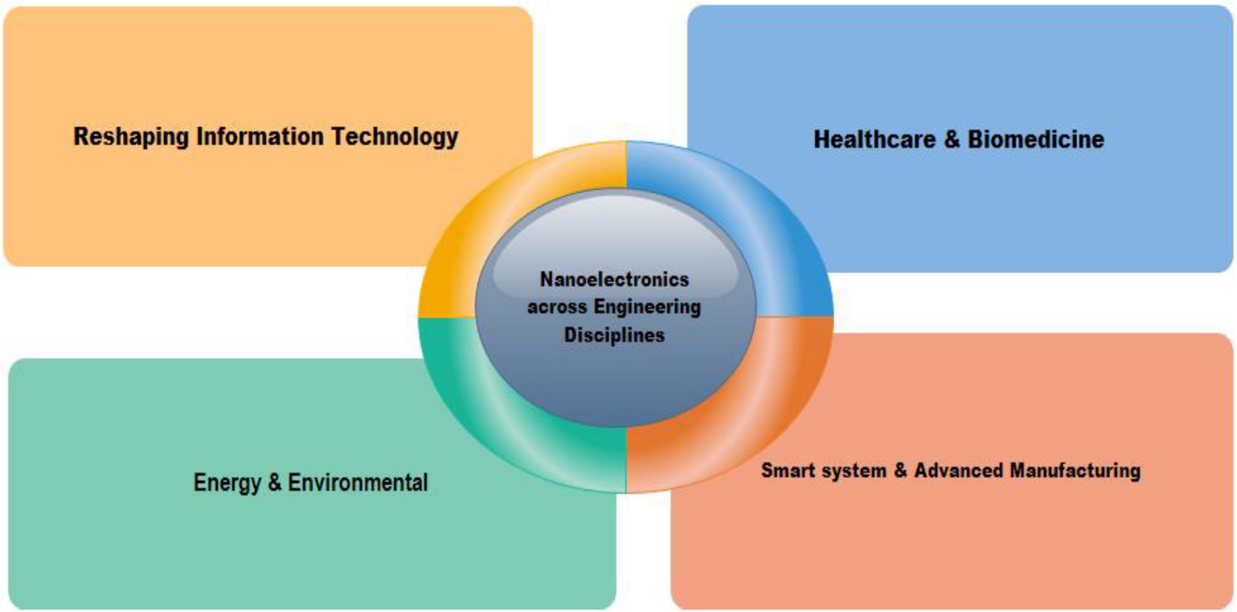
Figure 2. Nanoelectronics applications.
Advanced CMOS and beyond-CMOS logic devices
FinFETs and all-around gate transistors are examples of commercial semiconductor technologies based on nanoelectronic design principles (22). They offer enhanced electrostatic control and significantly reduce the short channel effects. Such devices are mature and comprise the fully developed examples of nanoelectronics. In contrast, beyond CMOS devices such as tunnel field-effect transistor (FET), nanosheet transistors, and negative capacitance FETs are largely experimental at present due to their difficulty in fabrication, unreliability, and high variability.
Memory technologies and data storage
Nanoelectronics has been very successful in significantly improving memory technologies such as resistive RAM, phase change memory, and magnetic RAM. These new devices store data by using nanoscale material phase changes, spin-dependent transport, or filamentary conduction and are non-volatile and very dense (23). While some of the technologies have been commercialized, there are still problems with endurance, retention, and large-scale manufacturing that need to be addressed.
Quantum and neuromorphic computing
Quantum computing and neuromorphic architectures are two revolutionary fields of research enabled by nanoelectronics (24). Quantum devices rely on nanoscale control of qubits, while neuromorphic systems use memristive and synaptic-like devices to emulate neural computation (25). Despite a great deal of progress in research, the two paradigms still have very significant issues to resolve, including error correction, heat management, device variability, and system-level integration. Thus, they are only at the scale of small demonstrations in laboratories.
Biomedical and healthcare applications
Nanoelectronics has introduced unprecedented sensitivity and functionality into biomedical systems by enabling electronic interaction at cellular and molecular length scales.
Nanoelectronic biosensors and diagnostics
Nanoelectronic biosensors typically employ nanoscale transducers that can detect biomolecules even in extremely low concentrations that can signal disease at its earliest phase and can track in real time. Examples are biosensors based on FET and nanopores that demonstrate such potential (26). While some wearable diagnostic platforms are nearly market-ready, issues with long-term stability, reproducibility, and calibration still pose significant challenges.
Therapeutic, implantable, and biointegrated systems
Implantable nanoelectronic systems can literally communicate with the nervous system, release targeted drugs, and perform closed-loop medical interventions. They incorporate nanoscale electronics with biological tissue, thus complicating the acquisition of regulatory approval, power delivery, signal stability, and safety considerations for living things (27). Most of these types of technologies are still at the clinical or preclinical research early stages. Figure 3 depicts the usage of these nanotechnologies in various sectors. Along with this, the figure reveals major barriers, privacy problems, and ethical issues that call for very careful handling.

Figure 3. Navigating the landscape of nanoelectronics in various fields.
Energy and environmental systems
Nanoelectronics plays an increasingly important role in addressing global challenges related to energy generation, storage, and environmental monitoring.
Photovoltaic and energy-harvesting devices
Materials engineered at the nanoscale make a significant contribution to improvements in light absorption, charge separation, and carrier transport in photovoltaic devices. At the lab scale, quantum dots, nanowires, and nanostructured coatings have all shown a positive impact on efficiency (28). Nevertheless, issues of durability over time, the possibility of large-scale production, and the affordability of these technologies are still holding back their commercial use.
Energy storage and environmental monitoring
Nanoelectronics makes advanced energy storage possible through the use of nanostructured electrodes of batteries and supercapacitors to enhance capacity and charge/discharge rates (29). In environmental applications, nanoelectronic sensors allow the on-the-spot detection of pollutants and hazardous substances; however, the environmental impacts throughout the life cycle of nanomaterials need to be carefully evaluated.
Advanced manufacturing and automation
Nanoelectronics underpins the transition toward intelligent and adaptive manufacturing systems.
Smart manufacturing and industrial automation
Embedded nanoelectronic sensors and actuators in manufacturing environments allow for real-time monitoring, predictive maintenance, and adaptive control (30). Although individual components can be purchased in the market, the fully autonomous nano-integrated manufacturing ecosystems are mostly conceptual and, therefore, still need technological development.
Challenges, ethics, and regulatory landscape
Technical and economic barriers
Some of the main difficulties are in scaling, performance of individual devices, variability, and intricacy of integration. The industries are also trapped with large upfront investments and limited access to intellectual property, which further hinders the commercialization process. As can be seen from Figure 4, these industries face major technological challenges in their effort to tap the enormous potential of nanoelectronics in the future.

Figure 4. Technical hurdles.
Ethical, environmental, and societal considerations
Nanotoxicity, data privacy, and cybersecurity risks require designers to be proactive by ethics and design by security approaches, which ethical and security regulatory frameworks should further support. Therefore, to enable responsible expansion as well as integration, invention has to continue simultaneously with ethics awareness, community welfare, and community safety, thus cautiously navigating nanotechnology and human civilization intersections, as shown in Figure 5.

Figure 5. Societal and ethical impact of nanotechnology.
Workforce development and policy needs
Interdisciplinary education and coordinated policy initiatives are essential to ensure responsible and equitable development of nanoelectronics.
Conclusion and future outlook
Nanoelectronics is a change in direction from scaling driven technological development to physics enabled innovation. In the future, its impact will mainly hinge on continuous enhancements in materials, manufacturing, and system integration, and the responsible governance and ethical oversight. If developed and used responsibly, nanoelectronics might be a mature engineering platform that offers real benefits to society in many areas.
Conflict of interest
The authors declare that the research was conducted in the absence of any commercial or financial relationships that could be construed as a potential conflict of interest.
References
1. Gargini P, Balestra F, Hayashi Y. Roadmapping of nanoelectronics for the new electronics industry. Appl Sci. (2021) 12(1):308. doi: 10.3390/app12010308
2. Li S. From Moore’s law to function density law. In: Li S editor. MicroSystem Based on SiP Technology. Singapore: Springer (2022). p. 3–27. doi: 10.1007/978-981-19-0083-9_1
3. Alfieri A, Anantharaman SB, Zhang H, Jariwala D. Nanomaterials for quantum information science and engineering. Adv Mater. (2023) 35(27):2109621. doi: 10.1002/adma.202109621
4. Donarini A, Grifoni M. Quantum Transport in Interacting Nanojunctions. Cham: Springer (2024). doi: 10.1007/978-3-031-55619-7
5. Kanrar SS, Das SS, Sarkar SK. 6 Classical to semiclassical transport in field effect transistors. In: Kumar N, Kumar P, Dixit A, Singh P editors. Classical to Quantum Transport in Multi-Dimensional Field Effect Transistors. Boca Raton, FL: CRC Press (2025).
6. Li Q, Wu K, Zhu H, Yang Y, He S, Lian T. Charge transfer from quantum-confined 0D, 1D, and 2D nanocrystals. Chem Rev. (2024) 124(9):5695–763. doi: 10.1021/acs.chemrev.3c00742
7. Alshebly W, Shalchian M, Shafizade D, Chalechale A, Jazaeri F. Transcapacitances modeling in ultra-thin gate-all-around junctionless nanowire FETs, including 2D quantum confinement. Solid-State Electron. (2023) 200:108544. doi: 10.1016/j.sse.2022.108544
8. Thureja D, Imamoglu A, Smoleński T, Amelio I, Popert A, Chervy T et al. Electrically tunable quantum confinement of neutral excitons. Nature. (2022) 606(7913):298–304. doi: 10.1038/s41586-022-04634-z
9. Chen Z, Manian A, Widmer-Cooper A, Russo SP, Mulvaney P. Semiconductor quantum dots in the cluster regime: focus review. Chem Rev. (2025) 125(9):4359–96. doi: 10.1021/acs.chemrev.4c00967
10. Liu F, Fan Z. Defect engineering of two-dimensional materials for advanced energy conversion and storage. Chem Soc Rev. (2023) 52(5):1723–72. doi: 10.1039/D2CS00931E
11. Kolahdouz M, Xu B, Nasiri AF, Fathollahzadeh M, Manian M, Aghababa H et al. Carbon-related materials: graphene and carbon nanotubes in semiconductor applications and design. Micromachines. (2022) 13(8):1257. doi: 10.3390/mi13081257
12. Thomas RM, Mishra A, Shahin S, Khan MS, Khan ZH. Advanced nanomaterials in electrical and electronics miniaturization. In: George SC, Tawiah B, Jacob M, Haponiuk J editors. Advanced Nanomaterials and Composites. (Vol. 1), Singapore: Springer (2026). p. 157–219. doi: 10.1007/978-981-95-3600-9_6
13. Tang D-M, Cretu O, Ishihara S, Zheng Y, Otsuka K, Xiang R et al. Chirality engineering for carbon nanotube electronics. Nat Rev Electr Eng. (2024) 1(3):149–62. doi: 10.1038/s44287-023-00011-8
14. Mondal J, Lamba R, Yukta Y, Yadav R, Kumar R, Pani B et al. Advancements in semiconductor quantum dots: expanding frontiers in optoelectronics, analytical sensing, biomedicine, and catalysis. J Mater Chem C. (2024) 12(28):10330–89. doi: 10.1039/D4TC01396D
15. Selvaraj S, Chauhan A, Verma R, Viswanathan K, Subbarayan R, Ghotekar S. Multifunctional biomedical applications of MXene-based hydrogels: a review. Inorganic Chem Commun. (2024) 164:112457. doi: 10.1016/j.inoche.2024.112457
16. Merkel TJ, Herlihy KP, Nunes J, Orgel RM, Rolland JP, DeSimone JM. Scalable, shape-specific, top-down fabrication methods for the synthesis of engineered colloidal particles. Langmuir. (2010) 26(16):13086–96. doi: 10.1021/la903890h
17. Pisco M, Galeotti F. Nano-and micropatterning on optical fibers by bottom-up approach: the importance of being ordered. Appl Sci. (2021) 11(7):3254. doi: 10.3390/app11073254
18. Wen B, Yang J, Hu C, Cai J, Zhou J. Top-down fabrication of ordered nanophotonic structures for biomedical applications. Adv Mater Interfaces. (2024) 11(5):2300856. doi: 10.1002/admi.202300856
19. Hirschi S, Ward TR, Meier WP, Müller DJ, Fotiadis D. Synthetic biology: bottom-up assembly of molecular systems. Chem Rev. (2022) 122(21):16294–328. doi: 10.1021/acs.chemrev.2c00339
20. Palagati S, Kudamala RR, Satyanarayana SV, Veeram JR, Garg T, Parihar A et al. Advanced materials synthesis by top-down and bottom-up approaches. In: Gaikwad MU, Parihar A, Khan R editors. Advanced Materials. Boca Raton, FL: CRC Press (2024). p. 201–21.
21. Bespalov V, Dyuzhev N, Kireev VY. Possibilities and limitations of CMOS Technology for the production of various microelectronic systems and devices. Nanobiotechnol Rep. (2022) 17(1):24–38. doi: 10.1134/S2635167622010037
22. Das D, Gurung S, Singh M, Chaudhary T, Raj B. FinFET and its application. In: Raj B, Tripathi SL, Chaudhary T, Singh M editors. Nanoelectronics: Materials to Chips Design. Boca Raton, FL: CRC Press (2025). p. 31–53.
23. Das RS. Emerging memory technologies: a systematic literature review with focus on resistive RAM (RRAM) and phase-change memory (PCM). J Sci Eng Res. (2022) 9(6):53–61.
24. ul Haq MI, Hassan NU, Rizvi DQ. Nano-scale architectures for quantum ai robotics: a review of emerging trends in neuromorphic chip design, advanced medical diagnostics, and cybernetic enhancements. Spectr Eng Sci. (2025) 3(10):1563–96. doi: 10.5281/zenodo.17621252
25. Prati E. Atomic scale nanoelectronics for quantum neuromorphic devices: comparing different materials. Int J Nanotechnol. (2016) 13(7):509–23. doi: 10.1504/IJNT.2016.078543
26. Ramesh M, Janani R, Deepa C, Rajeshkumar L. Nanotechnology-enabled biosensors: a review of fundamentals, design principles, materials, and applications. Biosensors. (2022) 13(1):40. doi: 10.3390/bios13010040
27. Zheng Z, Zhu R, Peng I, Xu Z, Jiang Y. Wearable and implantable biosensors: mechanisms and applications for closed-loop therapeutic systems. J Mater Chem B. (2024) 12:8577–604. doi: 10.1039/D4TB00782D
28. Ma J, Sabzehparvar M, Pan Z, Tagliabue G. Nanostructured Fe2O3/CuxO heterojunction for enhanced solar redox flow battery performance. J Mater Chem A. (2025) 13(2):1320–9. doi: 10.1039/D4TA06302C
29. Roy DB, Das S. Advanced nanostructured materials for energy storage devices. In: Singh L editor. Design, Fabrication, and Significance of Advanced Nanostructured Materials. Hershey, PA: IGI Global (2025). p. 187–206. doi: 10.4018/979-8-3693-5320-2
30. Hamida B, Jacob G. Nanotube-based sensors and actuators for smart manufacturing systems. In: Deshwal D, Narwal AK, Srivastava V, Babbar A, Weaver JM editors. Nanomaterials for Smart Manufacturing. Boca Raton, FL: CRC Press (2026). p. 290–319.
© The Author(s). 2026 Open Access This article is distributed under the terms of the Creative Commons Attribution 4.0 International License (https://creativecommons.org/licenses/by/4.0/), which permits unrestricted use, distribution, and reproduction in any medium, provided you give appropriate credit to the original author(s) and the source, provide a link to the Creative Commons license, and indicate if changes were made.